Advanced Packaging Market Research, 2032
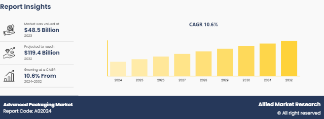
The Global Advanced Packaging Market was valued at $48.5 billion in 2023, and is projected to reach $119.4 billion by 2032, growing at a CAGR of 10.6% from 2024 to 2032.

Market Introduction and Definition
Advanced packaging is a supporting case that prevents physical damage and corrosion to silicon wafers, logic units and memory, during the final stage of semiconductor manufacturing process. It allows the chip to be connected to a circuit board. In addition, advanced packaging involves grouping distinct techniques including 2.5D, 3D-IC, fan-out-wafer-level packaging and system-in-package.
Key Takeaways
On the basis of type, the CSP flip chip ball grid array segment dominant the market in terms of revenue in 2023 and is anticipated to grow at the fastest CAGR during the forecast period.
On the basis of end user, the consumer electronics segment dominated the advanced packaging market size in terms of revenue in 2023.
Region-wise, Asia-Pacific generated the largest revenue in 2023 and is anticipated to grow at the highest CAGR during the forecast period.
Industry Trends:
In August 2023, Taiwan Semiconductor Manufacturing Company (TSMC) announced investing 90 billion New Taiwan dollars to build an advanced chip packaging plant in Taiwan amid booming global demand. Additionally, Micron stated in June 2023 that it would spend millions of dollars on a factory in China despite the Chinese government having just deemed its goods a security risk. Over the coming years, Micron stated it will upgrade its chip packaging factory in Xi'an with investments totaling YUAN 4.3 billion (slightly over USD 600 million) .
In July 2023, Amkor Technology extensively detailed its efforts and achievements in developing and validating wire bond and flip chip packaging for devices manufactured using TSMC's advanced low-k process technologies. Collaborating with multiple clients on low-k product qualification, Amkor aimed for a substantial volume ramp-up in low-k packages during the latter half of the year.
In November 2022, Intel Corporation commenced work on a new semiconductor assembly and testing facility in Penang. Comprising two buildings (Plants 4 and 5) totaling 982, 000 square feet within the Bayan Lepas Free Industrial Zone, this facility, expected to be finalized by 2025, was anticipated to generate 2, 700 job opportunities within the local market.
Key market dynamics
Increase in demand for miniaturization of devices is a significant driver for the advanced packaging market. With increase in advancement in technologies, manufacturers are laying emphasis in providing compact electronic devices in various industry verticals such as consumer electronics, healthcare, automotive, and semiconductor IC manufacturing. These manufacturers are reducing the size of the integrated circuits to ensure fine patterning on the wafers and chips. In addition, the medical devices industry has witnessed an increase in demand for nano-sized robotic surgery equipment with sophistication and advances into wearable and personalized healthcare gadgets. Therefore, the trends toward compact electronic devices have created the need for designers to outgrow the conventional packaging solutions and to adopt advanced packaging. Miniaturized electronic devices are experiencing growth in the semiconductor industry due to a rise in demand for high-performance electronics. Moreover, the rise in developments of technologies such as RFID, MEMS devices, and other power devices boost the demand for thin wafers. For instance, wafer back grinding process is utilized to reduce the thickness of wafers from 750 μm to around 75-50 μm. Thin wafers help reduce the thickness of packages, especially for smartphones, handheld devices, and compact electronic products.
However, high initial costs pose a substantial barrier to the widespread adoption of advanced packaging systems. Advanced packaging is a very costly process as against conventional packaging solutions used in semiconductor industry. The cost of designing and manufacturing chips at each new node is costly at certain levels. In addition, the cost of wafer fabrication is much higher due to the complexities of the ICs. Packaging of different chips and ICs with complex pattering increases the overall cost of advanced packaging and hampers its adoption. Advanced packaging comes with a lot of features such as easy and wider interconnections for chips and wafers and availability of heterogenous integration which makes it very viable in the semiconductor industry. However, due to the availability of such features, the cost of advanced packaging over conventional packaging is quite high and makes it difficult for small manufacturers to adopt this technology. Therefore, high cost associated with advanced packaging solutions as a major restraint, hampers the growth of the advanced packaging market globally.
Furthermore, the emerging trends of fan-out wafer level packaging present significant opportunities for the advanced packaging market. Fan-out wafer level packaging is an integrated circuit packaging technology and is also an enhancement of standard wafer-level packaging solutions. As against conventional packaging solutions in which a wafer is diced first, fan-out wafer level packaging involves packaging of integrated circuits while still being a part of the wafer and is diced afterwards. Fan-out wafer level packaging provides smaller package footprint along with improved thermal and electrical performances as compared to conventional packages. In addition, fanout wafer level packaging promotes high number of wafer contacts without increasing the die size. There are various significant factors that lead toward the adoption of technology on the global front. These include elimination of wafer bumping, elimination of flip-chip reflows, better wafer-level yield, embedded integration of passive devices, and easier adoption of system-in-package and 3D integrated circuits packaging. These features promote the adoption of fan-out level packaging in the advanced packaging solutions and offer lucrative opportunities for the growth of the market globally.
Patent Analysis of Global Advanced Packaging Market
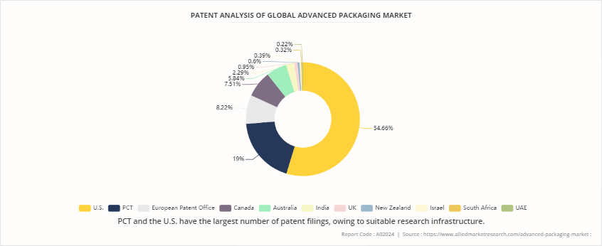
The global Advanced Packaging Market is segmented according to the patents filed in U.S. Patent Corporation Treaty (PCT) , China, Republic of Korea, European Union, Germany, the UK, Canada, and Australia. PCT and the U.S. have the largest number of patent filings, owing to suitable research infrastructure. Approvals from these authorities are accepted by devices registration authorities in many developing countries. Therefore, China and U.S. have the maximum number of patent filings. Moreover, the majority of companies belong to China, which largely contributes toward growth of the number of patent applications filed in the region.

Market Segmentation
The advanced packaging industry is segmented into type, end user, and region. By type, it is divided into flip chip CSP, flip-chip ball grid array, wafer level CSP, 2.5D/3D, fan-out WLP, and others. By end user, it is classified into consumer electronics, automotive, industrial, healthcare, aerospace & defense, and others. Region wise, the advanced packaging market trends are analyzed across North America, Europe, Asia-Pacific, and LAMEA.
Market Segment Outlook
By type, the CSP Flip chip ball grid array segment dominant the market in terms of revenue in 2023 and is expected to follow the same trend during the forecast period due to its superior performance and efficiency. Flip chip ball grid array offers excellent electrical and thermal performance, making it ideal for high-performance computing and mobile devices. It enables higher interconnection density, improved signal integrity, and better heat dissipation, which are critical for advanced semiconductor applications. The rising demand for miniaturized, high-performance electronic devices and the continuous advancements in semiconductor technology further drive the adoption of CSP Flip chip ball grid array packaging solutions.
By end user, the consumer electronics segment held the highest market share in 2023, for the advanced packaging market share due to the surging demand for compact, high-performance electronic devices such as smartphones, tablets, and wearables. Advanced packaging technologies, such as Fan-Out Wafer-Level Packaging (FOWLP) and Through-Silicon Via (TSV) , enable enhanced functionality, miniaturization, and improved power efficiency, whichare essential for modern consumer electronics. Additionally, the rapid adoption of technologies like 5G, IoT, and AI in consumer devices necessitates advanced packaging solutions to support higher processing speeds and integration densities, further driving market growth in this segment.
Regional/Country Market Outlook
On the basis of region, the advanced packaging market forecast is analyzed across North America, Europe, Asia-Pacific, and LAMEA. Asia-Pacific held the highest market share in the advanced packaging market in 2023 due to its strong semiconductor manufacturing base, significant investments in R&D, and the presence of major industry players. Moreover, advanced packaging market size by Country like China, Taiwan, South Korea, and Japan lead in semiconductor production and innovation, driven by high demand from consumer electronics, automotive, and telecommunications sectors. In addition, favorable government policies, robust supply chains, and the region's role as a global electronics manufacturing hub contribute to the growth of advanced packaging technologies. The rapid adoption of 5G, IoT, and AI further fuels the demand for sophisticated packaging solutions in the region. For instance, In December 2022, China announced its commitment to a support package exceeding YUAN 1 trillion (USD 143 billion) for its semiconductor industry. This initiative is a crucial step towards achieving self-sufficiency in chip production and is a response to U.S. actions aimed at hindering China's technological progress. The demand for packaging services is anticipated to rise considerably during the forecast period, owing to the region's intensified efforts to enhance domestic chip manufacturing.
Competitive Landscape
The major advanced packaging manufacturer operating in the market are Amkor Technology, Intel Corporation, Qualcomm Technologies Inc., Taiwan Semiconductor Manufacturing Company, IBM, Microchip Technology, Renesas Electronics Corporation, Texas Instruments, and Analog Devices.
Recent Key Strategies and Developments
In June 2023, Amkor Technology Inc., a leading provider of semiconductor packaging and test services, is at the forefront of innovating advanced packaging to enable the car of the future. The evolution of the enhanced automotive experience has been dramatic over the past few years, reflected in the surge of car-related semiconductor sales. With over 40 years of automotive experience and a broad geographic footprint supporting global and regional supply chains, Amkor is well-positioned to capture growth from the increasing semiconductor content in vehicles. As a frequent automotive OSAT, Amkor leverages its expertise to support the accelerating demands of the automotive industry.
Key Sources Referred
Semiconductor Industry Association (SIA)
SEMI
IEEE Electron Devices Society (EDS)
U.S. Department of Energy
Global Semiconductor Alliance (GSA)
World Economic Forum
European Semiconductor Industry Association (ESIA)
Key Benefits For Stakeholders
- This report provides a quantitative analysis of the market segments, current trends, estimations, and dynamics of the advanced packaging market analysis from 2024 to 2032 to identify the prevailing advanced packaging market opportunities.
- The market research is offered along with information related to key drivers, restraints, and opportunities.
- Porter's five forces analysis highlights the potency of buyers and suppliers to enable stakeholders make profit-oriented business decisions and strengthen their supplier-buyer network.
- In-depth analysis of the advanced packaging market segmentation assists to determine the prevailing market opportunities.
- Major countries in each region are mapped according to their revenue contribution to the global market.
- Market player positioning facilitates benchmarking and provides a clear understanding of the present position of the market players.
- The report includes the analysis of the regional as well as global advanced packaging market trends, Advanced Packaging Company List, Advanced Packaging Market Share by Companies, Advanced Packaging Industry Report, Advanced Packaging Sector Analysis, Semiconductor Advanced Packaging, Advanced Packaging Technology key players, market segments, application areas, and market growth strategies.
Advanced Packaging Market Report Highlights
| Aspects | Details |
| Market Size By 2032 | USD 119.4 Billion |
| Growth Rate | CAGR of 10.6% |
| Forecast period | 2024 - 2032 |
| Report Pages | 250 |
| By Type |
|
| By End User |
|
| By Region |
|
| Key Market Players | IBM Corporation, Intel Corporation., microchip technology, Qualcomm Technologies Inc., TAIWAN SEMICONDUCTOR MANUFACTURING COMPANY LIMITED, Amkor Technology Inc., Renesas Electronics Corporation, Texas Instruments Inc., Analog devices |
5G Deployment and Expansion, and Expansion in Industrial IoT are the upcoming trends of advanced packaging market in the globe.
consumer electronics is the leading application of Advanced Packaging Market
Asia-Pacific is the largest regional market for Advanced Packaging
In 2023, $45.50 billion was the estimated industry size of advanced packaging
Amkor Technology, Intel Corporation, Qualcomm Technologies Inc., Taiwan Semiconductor Manufacturing Company, IBM, Microchip Technology, Renesas Electronics Corporation, Texas Instruments, and Analog Devices. are the top companies to hold the market share in Advanced Packaging
Loading Table Of Content...


