Wafer Level Packaging Market Research, 2030
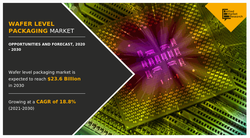
The global wafer level packaging market size was valued at $4.5 billion in 2020, and is projected to reach $23.6 billion by 2030, growing at a CAGR of 18.8% from 2021 to 2030. Wafer level packaging (WLP) is a method of attaching packaging components to an integrated circuit (IC) prior to dicing the wafer. This procedure varies from a traditional method, which involve slicing the wafer into separate circuits (dice) before attaching the packaging components.
Growth of the global wafer level packaging industry is anticipated to be driven by factors such as rise in adoption of high-speed, compact size, and less expensive electronic products. In addition, wafer level packaging’s technological superiority over traditional packaging techniques and the impending need of circuit miniaturization in microelectronic devices boost the market growth. However, complexities in manufacturing process act as major restraint for the market. On the contrary, rise in use of wafers in the automotive industry is expected to fuel the market growth during the forecast period.
Segment Overview
The wafer level packaging market is segmented into Technology, Type and End User.
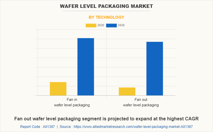
By technology, the market is classified into fan in wafer level packaging and fan out wafer level packaging. Depending on type, it is categorized into 3D TSV WLP, 2.5D TSV WLP, WLCSP, Nano WLP, and others.
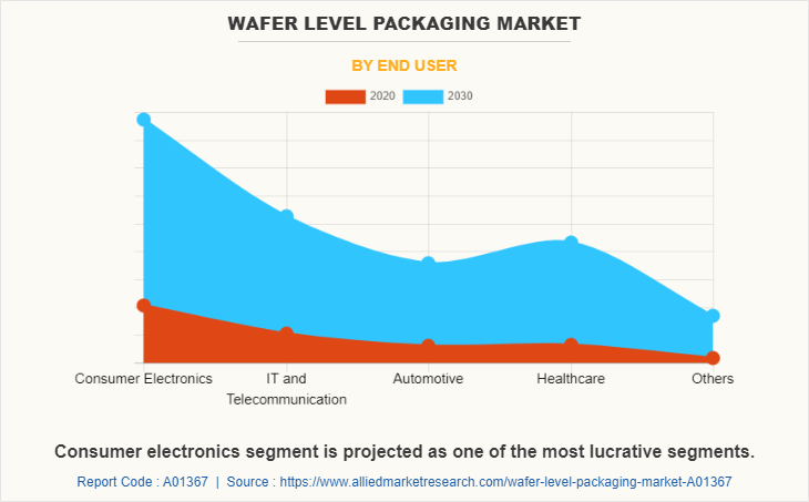
On the basis of end user, the market is divided into consumer electronics, IT & telecommunication, automotive, healthcare, and others.
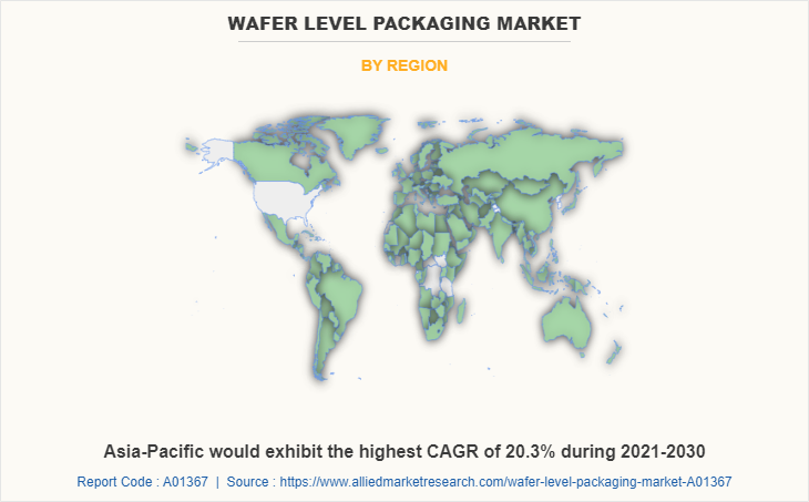
By region, the wafer level packaging market trends are analyzed across North America (U.S., Canada, and Mexico), Europe (UK, Germany, France, and rest of Europe), Asia-Pacific (China, Japan, Taiwan, India, South Korea, and rest of Asia-Pacific), and LAMEA (Latin America, the Middle East, and Africa). Asia-Pacific dominated the wafer level packaging market in 2020, and is projected to register significant growth rate during the forecast period,owing to growth in the automotive segment. Furthermore, Asia-Pacific is expected to witness significant growth by the end of the forecast period, followed by LAMEA.
Leading wafer level packaging industry manufacturers such as Applied Materials Inc, Qualcomm Technologies Inc, Amkor Technology Inc, and Jiangsu Changjiang Electronics Technology Co Ltd are focused on their investments on technologically advanced, cost-effective, and more secure products & solutions for various applications. Also, In semiconductor advance packaging sector wlcsp package, wlcsp process flow, and wafer chip scale package are in the latest trends.
Top Impacting Factors
The prominent factors that impact the wafer level packaging market growth include rapid development in the semiconductor industry, high adoption of consumer electronics devices, and increase in demand for ultra-thin wafers. In addition,surge in Internet of Things (IoT) technologyfuels the market growth. However, high initial investment restricts the market growth. On the contrary, rise in investment in wafer fabrication equipment and materialsis expected to create lucrative opportunities for the market.
Competition Analysis
Competitive analysis and profiles of the major wafer level packaging market playerssuch asAmkor Technology Inc, Applied Materials Inc, ASML Holding N.V, Deca Technologies, Fujitsu, Jiangsu Changjiang Electronics Technology Co Ltd, Lam Research Corporation, Qualcomm Technologies Inc, Tokyo Electron Ltd, and Toshiba Corporation have been covered in the report.
Key Benefits For Stakeholders
- This study comprises analytical depiction of the global wafer level packaging market size along with current trends and future estimations to depict imminent investment pockets.
- The overall wafer level packaging market analysis is determined to understand the profitable trends to gain a stronger foothold.
- The report presents information related to key drivers, restraints, and opportunities with a detailed impact analysis.
- The current wafer level packaging market forecast is quantitatively analyzed from 2020 to 2030 to benchmark the financial competency.
- Porter’s five forces analysis illustrates the potency of the buyers and the wafer level packaging market share of key vendors.
- The report includes the market trends and the market share of key vendors.
Wafer Level Packaging Market Report Highlights
| Aspects | Details |
| By Technology |
|
| By Type |
|
| By End User |
|
| By Region |
|
| Key Market Players | Applied Materials, Inc., Amkor Technology, Inc., Fujitsu, Qualcomm Technologies, Inc., Tokyo Electron Ltd., Jiangsu Changjiang Electronics Technology Co. Ltd, Lam Research Corporation, Toshiba Corporation, ASML Holding N.V, Deca Technologies |
Analyst Review
The global wafer level packaging market is flourishing at a rapid pace. However, high initial investment is still a concern for new entrants. Market players are generously investing in R&D activities to develop improved solutions to reduce the overall cost of wafer level packaging products. In addition, according to industry experts, it is essential to optimize affordable prices for wafer level packaging products for long-term growth.
In November 2021, Amkor Technology Inc. announced the business expansion of advanced packaging technology capacity with a new factory setup in Bac Ninh, Vietnam. This is expected to provide a long-term investment in geographical diversification and factory capacity expansion, supporting Amkor’s commitment to reliable supply chain solutions for its customers.
Key players of the market focus on introducing technologically advanced products to remain competitive in the market. Partnership, acquisition, and product launches are expected to be the prominent strategies adopted by the market players. Asia-Pacific accounted for a major share of the market in 2020, owing to the presence of major players in the region; Also, Asia-Pacific is expected to grow at the highest CAGR, owing to rise in adoption of wafer level packaging market in a variety of fields.
Asia-Pacific dominated the wafer level packaging market in 2020
The global wafer level packaging market size was valued at $4.54billion in 2020
asApplied Materials Inc, Qualcomm Technologies Inc, Amkor Technology Inc, and Jiangsu Changjiang Electronics Technology Co Ltd
It is widely used in PCB Design
Integration technology such as fan-in and fan-out are in the latest trend.
Loading Table Of Content...
